DS-A Lab 2: Combinational Circuits Part II
1Introduction
In this lab, you will create and test an SV description of a circuit that displays the numbers 0 to 7 on a 7-segment display. The inputs will be 8 switches labeled SW7 down to SW0. Assume only one switch is on at a time (one-hot encoding). The display should then show the number of the switch. For example, if you turn on switch SW3, the 7-segment display should show a 3.
A 7-segment display consists of 7 LEDs, which can be used to display numbers and a few letters. Figure 1 shows the 7-segment display with each LED segment labeled. Note that the LED controls are inverted! When a LED segment is controlled with a signal value of 0, it is on, and when it is controlled with a signal value of 1, it is off.
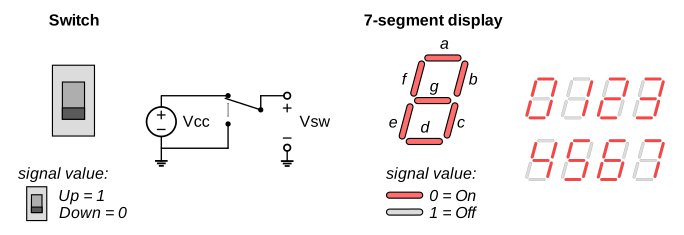
Figure 1:Information on the input switches and the output 7-segment display.
The circuit you’re going to implement is shown in Figure 2. The input switches are the blue signals on the left. The blue signals at the bottom go to the corresponding LEDs in Figure 1. Each LED is on for certain numbers, and off for others.
Here follows an explanation of how the circuit works. Please try to understand it in its entirety.
An encoder, assuming at most one switch is turned on, outputs the number of the switch that is on in binary. For example, if is on, then will be .
The encoder also outputs a signal . When none of the switches are on, , turning the output of all NAND gates on, meaning all LED segments are off (remember, their controls are inverted).
When a switch is on, , and the NAND gates act as inverters, inverting the output of the multiplexers, so e.g. in that case. The vector is used as a select signal for all 7 multiplexers.
The output of each multiplexer goes to one of the LED segments of the 7-segment display. For example, if is on, each multiplexer will output the signal value that is present at their port labeled .
In one of the homework assignments, you will determine what value should be present at every input of every multiplexer. Continuing the example, if is on, the signal value at port of the multiplexer whose output goes to LED segment , should be . Do you see why?
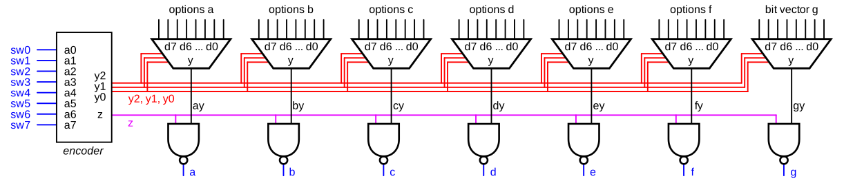
Figure 2:Block diagram of the full circuit.
As per usual, you are strongly recommended to prepare the following homework assignments before coming to the lab, to ensure you finish the lab on time.
2Homework
2.12A: 8-to-3 encoder
Given is the following truth table for a 8-to-3 encoder with input ports , , ... and output ports , , and :
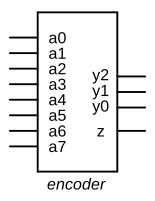
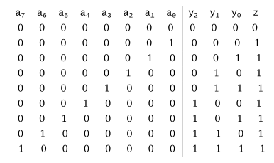
Go through the table and try to understand how the encoder works. Create logic expressions for the output ports , , and . Hint: Note that the table doesn’t contain all input combinations of , because it’s assumed at most one switch is on at a time. You can simplify your expression for the output ports by using OR gates only.
2.22B: 8:1 multiplexer
The logic expression for a 4:1 multiplexer with selection inputs and , data inputs , , , , and data output , is
Verify for yourself that this expression is correct. Create the logic expression for a 8:1 multiplexer with selection inputs , and , data inputs , , ... , and data output .
2.32C: 7-segment display
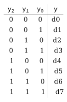
In Figure 2, there are 7 multiplexers. Each multiplexer outputs a signal , , , etc. These signals determine the color of each segment of the 7-segment display. The value should depend on which switch is selected, which is encoded by the the value of .
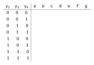
The signals are connected to the selection signals of each multiplexer. In the left table below, it is shown how the output of a multiplexer is detemined by one of its data inputs, depending on the values on its selection signals. Our task is to connect 0’s and 1’s to the data inputs , , , etc. of each multiplexer, such that each segment has the correct color for the switch that is selected, hence for the value of .
In the right table below, you can fill out what should be the values of the different data inputs for each multiplexer. For example, when the switch 3 is selected and number 3 should be displayed, and segment a (See Figure 1) should be on, so should be . So, below , on the line with , enter a . Using this logic, complete the right table below.
3Assignments
3.12A: 8-to-3 encoder
Use the logic expression of the 8-to-3 encoder to create a SystemVerilog description of the 8-to-3 encoder from homework assignment 2A. Use the module name encoder8. Use the testbench labsDSA/lab_2/encoder8_tb.sv to simulate the circuit in QuestaSim for 900 ns.
Let the result of the assignment be signed off by the TA now.
Once all assignments are checked off you receive a pass for this lab.
3.22B: 8:1 multiplexer
Use the logic expression of the 8:1 multiplexer to create a SystemVerilog of the 8:1 multiplexer from homework assignment 2B. Use the module name mux8. Use the testbench labsDSA/lab_2/mux8_tb.sv to simulate the circuit in QuestaSim.
Let the result of the assignment be signed off by the TA now.
Once all assignments are checked off you receive a pass for this lab.
3.32C: Switch to 7-segment display circuit
Create a structural SystemVerilog description of the complete circuit in Figure 2. Use the modules you wrote in the previous assignments. Call the top-level module switch2display. Use the entries of the truth-table of homework assignment 2C as values for the inputs , , .... d_0 of each multiplexer instance that controls a segment. You can just use signal values 1'b0 and 1'b1 at the relevant positions in the port map for the different multiplexer instances. E.g.
mux8 ix (1'b0, 1'b1, ....);Also create a testbench for the module switch2display, such that your QuestaSim simulation ends up looking like Figure 7.
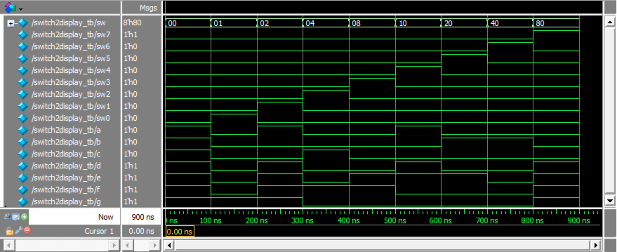
Figure 7:Correct simulation result for the switch2display circuit
Let the result of the assignment be signed off by the TA now.
Once all assignments are checked off you receive a pass for this lab.
3.42D: Implementation on FPGA
In the previous lab, we explained that there exist software tools that are able to interpret SystemVerilog code and create models of the circuits described in them. One such tool, QuestaSim uses these models to allow you to simulate your SV descriptions. Now, we’re going to use a different tool to “build” the circuit described in your SV code! There exist chips, like Field Programmable Gate Arrays (FPGAs), that you can program to behave like the circuit described in an SV description. In this assignment, you’re going to implement switch2display on an FPGA. By this we mean that you’re going to program an FPGA to behave like switch2display. The FPGA that we’re going to use is part of the Altera DE0 development board (See DE0 Board). Aside from the FPGA, this circuit board contains components like switches, leds, and much more to connect to the FPGA in order to test all sorts of circuits.
Familiarize yourself with the program Quartus by going through the tutorial in Quartus II. Quartus is a software tool that is able to program the FPGA on the Altera DE0 board to behave like your SV descriptions.
After you complete the Quartus tutorial, make sure to create a new project for the rest of this assignment.
In this case, we will not create a schematic for the circuit to be put on the FPGA, as was done in the tutorial, but we will use the SystemVerilog descriptions instead.
Use Project -> Add/Remove Files in Project ... to add the Verilog files for
encoder8,mux8andswitch2displayto the project.Click on the file with the module
switch2displayand select “Set as top-level entity”.Run Processing -> Start compilation
Assign the ports of the module
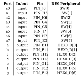
switch2displayto the FPGA pins as shown in Table 1.
Table 1:Pin mapping for switch to display converter
Rerun Processing -> Start compilation and next program the FPGA.
Test the working of the switch to display converter on the FPGA board.
Let the result of the assignment be signed off by the TA now.
Once all assignments are checked off you receive a pass for this lab.