Tutorial Quartus II
This appendix describes how to program the Altera FPGA using the Quartus II program. We will create a simple circuit diagram that contains a single inverter. The output signal of the inverter can be observed through a LED when we apply an input signal to the inverter through a push button.
Start the Quartus II program so that the window opens as shown in Figure 1.
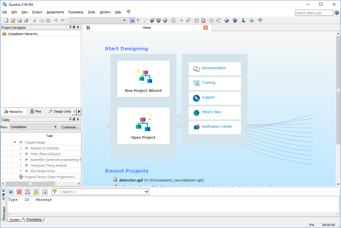
Figure 1:The Quartus II IDE
Like most IDE programs, also Quartus II is based on working with projects. Start by creating a new project using File > New Project Wizard. Enter the following information:
Working directory for this project: specify a map where you have write access, i.e. a map under the H: partition.
Name of this project: e.g. qtutorial
Name of the top-level design entity for this project: e.g. qtutorial
Then, click on Next. The window “Add Files” will open. No files will be added, so click on Next. The window “Family & Device Settings” will open. Select Cyclone III and EP3C16F484C6. Then, click on Finish
Now the schematic design can be made. Create a new worksheet by clicking on File > New and next selecting Block Diagram/Schematic File. Place an inverter on the work sheet by clicking the right mouse button, selecting Insert > symbol, selecting component ‘not’ under ../quartus/library/primitives/logic, clicking the OK button and finally placing the component in the middle of the worksheet.
Besides the ‘not’ component, also input and output labels need to be placed that deliver the input and output signals. The labels can be selected by clicking again with the right mouse button, selecting Insert > symbol, and then selecting either an ‘input’ component or an ‘output’ component under ../quartus/library/primitives/pin. Place one ‘input’ pin to the left of the inverter, and place two ‘output’ pins to the right of the inverter. Change the label names (by selecting the pin label, right clicking the mouse button and then selecting Properties) to ‘A’ for the input pin, and to ‘AINV’ and ‘ASAME’ for the ouput pins.
Use the Orthogonal Node Tool button to connect the input and output labels with wires to the inverter as shown in Figure 2. Save the file as qtutorial.bdf.
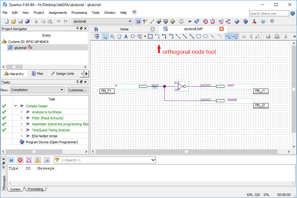
Figure 2:Inverter in the schematic window of Quartus
Now the pin assignment must be made. The pin assignment connects the input and output labels to the pins of the FPGA. First run a compilation using Processing > Start Compilation. Now the pins will be visible when you start the pin planner using Assignments > Pin Planner. Find the Node Name ‘A’ and fill in the location PIN_F1. This way A will be connected to the pin PIN_F1 of the FPGA, which is the pin that is connected to push button 2 on the FPGA board. For nodes ‘AINV’ and ‘ASAME’, respectively use locations PIN_J1 and PIN_J2 to respectively connect them to LED LEDG0 and LED LEDG1. See also Figure 3. For more information about pin numbers and pin connections, see DE0 Board.
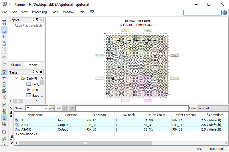
Figure 3:Editing the pin assignments
The entire design should now be recompiled. To compile click Processing > Start Compilation. Now the FPGA can be programmed. Click on Tools > Programmer. The programming window opens, see Figure 4. Make sure the USB-Blaster is selected in the Hardware Setup. By clicking on the Start button the FPGA will be programmed with the file qtutorial.sof, see Figure 4. Test if your FPGA works as you expected by pushing push button 2 and observing the behaviour of LEDs LEDG0 and LEDG1.
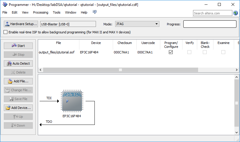
Figure 4:The Quartus Programmer Window