DS-A Lab 1: Combinational Circuits Part I
1Introduction
This lab consists of 3 parts. There exists a software tool called QuestaSim which can simulate the behavior of circuits described with SystemVerilog. In the first part of this lab, you will use QuestaSim to simulate a simple circuit. In the other parts, you will perform a few experiments to gain more insight in the behavior and design of combinational circuits.
2Homework
2.11A: QuestaSim Tutorial
Familiarize yourself with QuestaSim by going through the tutorial in the background material on Questasim.
2.21B.1: Logic Expressions
Determine the logic expressions for W, X, Y and Z in the circuit of Figure 1. Which logic function is realized with the circuit?
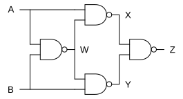
Figure 1:A circuit with NANDs
2.31B.2: Timing
The expressions of the assignment above give only the behavior in static condition. That is, the state that is finally reached after one or more inputs have changed. However, as we will see in this assignment, when going to the final state, temporarily transient effects (spikes) may occur at some nodes of the circuit.
Suppose that every gate has a gate delay time of tp = 10 ns (= 10-8 seconds). Complete the timing diagram of Figure 2 and indicate where spikes will occur.
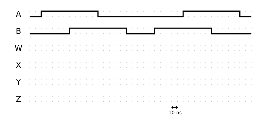
Figure 2:Timing diagram
2.41C: Design Combinational Circuit
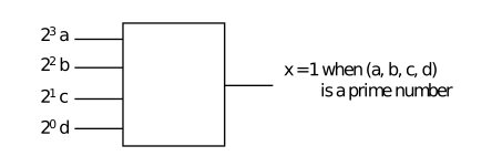
Figure 3:Prime number generator
This homework assignment prepares you to design a combinational circuit. The input is a 4-bit binary-coded number / vector that encodes the number sequence 0, 1, ..., 15. (See Figure 3) The output x should be 1 when the input represents a prime number, and 0 if not. Note that we don’t consider the numbers 0, 1, and 2 prime numbers. Complete the following steps:
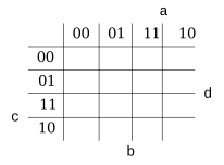
Write down the truth table and deduct a minimum sum of products for x with the following K-map.
Please read the tutorial (see background material on Espresso) on how to use the program ‘Espresso’.
Note: if you’re unable to install and run Espresso on your own computer, please perform the following steps during the course lab session in the Tellegen Hall.
Minimize the truth table with Espresso.
Compare the expression you found yourself with that of Espresso.
Espresso is a two-level minimization program, which means that the minimized circuit has two levels (AND and OR, apart from any inverters for the input signals). When we allow multiple levels (for example by doing factorisation on the minimum logical expression) we can further reduce the number of components and inputs.
3Assignments
3.11A: Introduction SV and QuestaSim
In this assignment we will describe a circuit in SV and simulate it with QuestaSim. The circuit realizes the AND function by connecting an inverter to the output of a NAND gate, as shown in Figure 5.
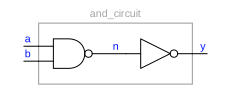
Figure 5:The AND circuit
Unzip labsDSA.zip (if you did not do so yet) and go to labsDSA/lab_1/a_introduction. The files you need in this assignment are and_circuit.sv and and_circuit_tb.sv. Go through the following steps:
Open the file
and_circuit.sv, and go to the module describing the AND circuit. Include the NAND gate and the inverter in the body of the module and map their ports to the ports of the AND circuit.Connect the output of the NAND gate to the input of the inverter via a local signal (let’s name it
n). Don’t forget to declare this signal!Add the AND circuit SV description and the provided testbench to a new QuestaSim project.
Compile the files, and run a simulation of 250 ns.
Let the result of the assignment be signed off by the TA now.
Once all assignments are checked off you receive a pass for this lab.
3.21B: Spikes
In homework assignment 1B.2, you completed the timing diagram of the circuit in Figure 1 with gate delays of zero and 10 ns. The presence of a gate delay was able to cause short pulses in the output signal. We call these short pulses “spikes”. In this assignment you will simulate the a SV description of the circuit in QuestaSim, and measure a physical copy of the circuit using a function generator and an oscilloscope in the Tellegen Hall.
Spikes in QuestaSim
Open the file labsDSA/lab_1/b_spikes/spikes.sv. The delay time chosen here for each NAND is 10 ns. Simulate this file for 400 ns using QuestaSim using the included testbench. Compare the results with your answer for homework assignment 1B.2.
Repeat the simulation, but now make the delay time of each NAND gate 1 ns instead of 10 ns. What happens to the spikes?
Spikes in Real Life
You’ve been provided with a PCB with the circuit on it. Connect the PCB to the function generator, power supply and oscilloscope as shown in Figure 6:
Use banana-clip cables to connect a power supply of 5V to the PCB: red for VCC and black for GND.
Apply a block signal (aka square wave) with a frequency of 100 kHz to input A. For the block signal, use the TTL output (0 - 5V) of the function generator and connect this output to the PCB with a BNC-clip cable.
Make B high by connecting it with a pin to pin wire to VCC.
Use the oscilloscope to check whether your prediction about spikes in signal X was correct. A probe cable should be used to connect the oscilloscope to the PCB. Check if the probe is set to 1x. Although this is not drawn in Figure 6, note that the ground connection of the function generator as well as the ground connection of the probe should both be connected to the ground connection of the circuit.
Let the result of the assignment be signed off by the TA now.
Once all assignments are checked off you receive a pass for this lab.
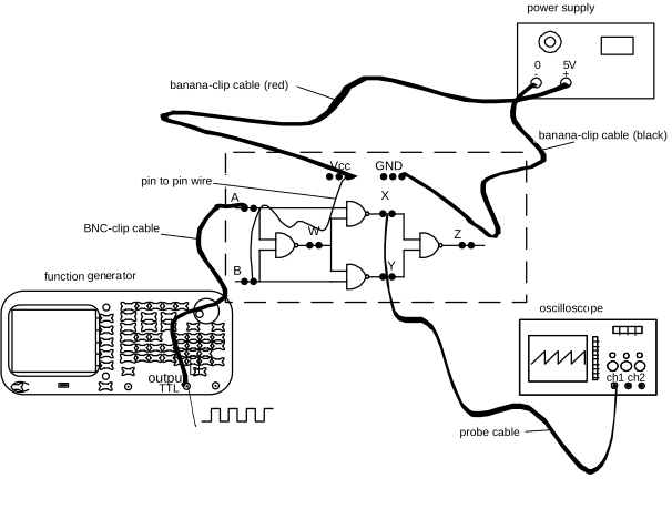
Figure 6:Connecting the PCB
3.31C: Minimization and implementation
Open the file labsDSA/lab_1/c_minimization. The file contains module descriptions of the following gates: a 2-input and a 4-input NAND gate, an inverter, and an XOR gate. The file also contains a module called prime, which is going to be an SV description of the prime circuit derived in homework assignment 1C.
If you didn’t use Espresso yet to minimize the truth table of the prime circuit (see homework assignment 1C), please do this first.
Convert the sum of products expression obtained from the K-map or from Espresso, to a NAND-NAND circuit. This requires 4 NANDs with 3 inputs, plus 3 inverters. Try this out.
Simplify the circuit further by taking an input variable from two product terms of the minimum sum of products out of parentheses, such that an expression results that is the product of that input variable and the XOR operation on the 2 other input variables. This introduces a third level, but the total number of components required for the circuit is reduced. Do this and check which components are now needed to realize the circuit.
A good design always starts with drawing the circuit (diagram) on paper. Draw the two circuits (the two-level NAND-NAND implementation and the three-level implementation with the XOR).
Now choose one of the two circuits to make a structural description in SystemVerilog. Use the file
prime.sv.Test the design with the supplied test bench (included as the module
prime_tbinprime.sv) in QuestaSim for 900 ns.
Let the result of the assignment be signed off by the TA now.
Once all assignments are checked off you receive a pass for this lab.