Vivado 2023.2 Tutorial
Introduction
In this tutorial you will make a circuit that makes an LED blink using an FPGA. Instead of soldering the circuit ourselves, we use a so-called “FPGA development board” (see Fig. 1), specifically the Basys3 board. The FPGA, highlighted in orange, comes in a Ball Grid Array (BGA) package (see Fig. 2). On a BGA package the input and output pins are metal balls arranged in a 2D array. Rows are labeled with letters and columns with numbers. E.g., pin D7 refers to the pin in the 4th column and the 7th row. Which pin is connected to which component on the board can be found in the Basys3 reference manual \cite{Basys3Reference}.

Figure 1:Top view of the Basys3 development board. (adapted from \cite{Basys3Reference})

Figure 2:Underside of the ARTIX-7 FPGA that is on the Basys3 board. (adapted from \cite{BasysFpgaPhoto})
The blinking LED circuit that you will make in this tutorial is shown in Fig. 3. Normally, the LED blinks at a frequency of 1 Hz with a 50% duty cycle.
The Basys3 board has a 100 MHz clock generation circuit that is connected to pin W5.
Switch 0 / SW0 (connected to pin V17) resets the circuit when high.
Switch 1 / SW1 (connected to pin V16) halves the duty cycle of the LED pulse to 25% when high.
LED 0 (connected to pin U16) is used as the output.

Figure 3:Diagram of the blinking LED circuit.
The FPGA needs to be configured to behave like a pulse generator for the LED. To do this, the manufacturer of the FPGA (Xilinx) created a software tool called Vivado. The user can supply Vivado with a circuit description in HDLs like SystemVerilog and VHDL, and Vivado will generate an FPGA configuration file to program the FPGA to behave like the supplied circuit description.
Before you can configure the FPGA, Vivado needs to go through a few steps:
Synthesis: The HDL description of the circuit is interpreted and converted into a hardware model.
Implementation: The synthesized model is converted into a circuit using the blocks and wires on the FPGA.
Bitstream generation: A file is generated which, if programmed on the FPGA, will connect the logic blocks on the FPGA according to the circuit from the implementation step.
The step-by-step tutorial in the next section will guide you through these steps.
Step-by-Step Tutorial
Step 1: Before we begin
Create a folder on your computer for this tutorial called “tutorial_vivado”.
Download the following files from Brightspace and move them into the folder “tutorial_vivado”:
blinking_led.sv: The SystemVerilog circuit description of the LED pulse generation circuit.
blinking_led_tb.sv: Its corresponding testbench.
Read the code of “blinking_led.sv” to see how it works. Refer to section Introduction for a description of the inputs and outputs.
(optionally) Simulate the circuit using the testbench in QuestaSim for 2 seconds. Note that a simulation of such length could take a few minutes to complete.
Step 2: Create a Vivado Project
Open Vivado 2023.2. You should be greeted with the screen in Fig. 4.
Click on Create Project >. A wizard will open. Press Next > to go to the first step.
The blinking LED circuit that you will make in this tutorial is shown in Fig. 3. Normally, the LED blinks at a frequency of 1 Hz with a 50% duty cycle.
The Basys3 board has a 100 MHz clock generation circuit that is connected to pin W5.
Switch 0 / SW0 (connected to pin V17) resets the circuit when high.
Switch 1 / SW1 (connected to pin V16) halves the duty cycle of the LED pulse to 25% when high.
LED 0 (connected to pin U16) is used as the output.
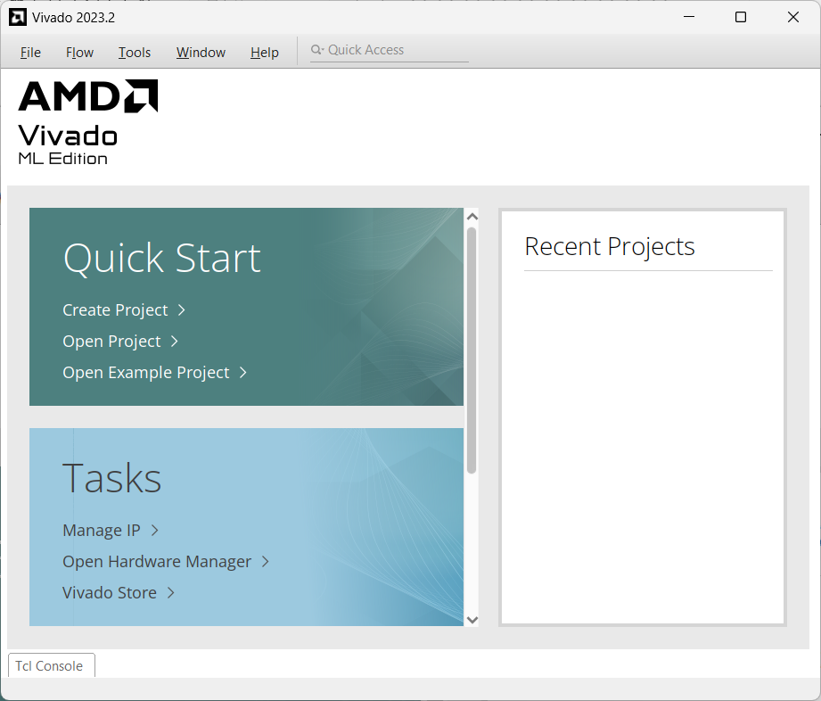
Figure 4:Vivado welcome screen
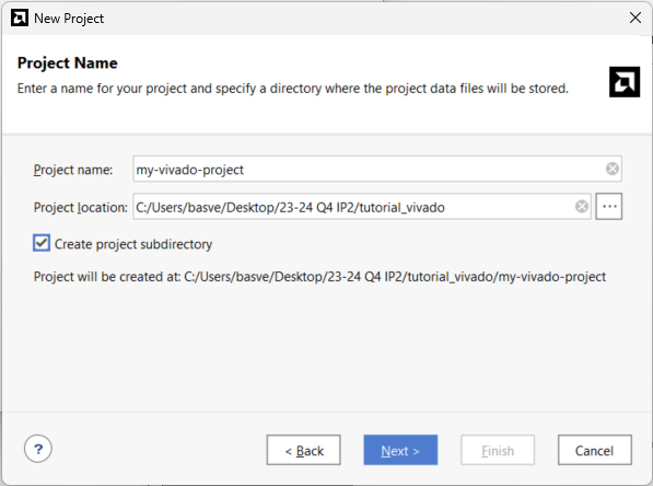
Name your project “my-vivado-project”.
Select “tutorial_vivado” as the project location.
Check Create project subdirectory to let Vivado create a folder called “my-vivado-project” in “tutorial_vivado”. All files Vivado will generate will be saved in the subfolder “my-vivado-project”.
Press Next >.
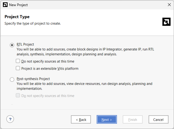
Select RTL Project as the project type. RTL stands for “Register Transfer Level”: A commonly used abstraction of synchronous digital circuits.
Press Next >.
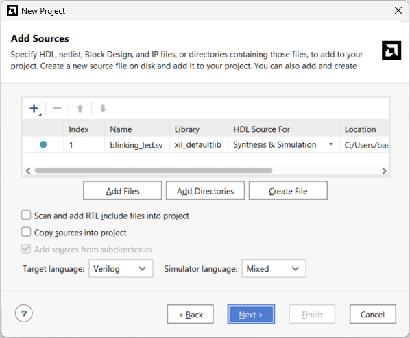
Click the + sign to add the file “blinking_led.sv” to the Vivado project.
Press Next >.
Skip this step for now. We will come back to this later.
Press Next >.
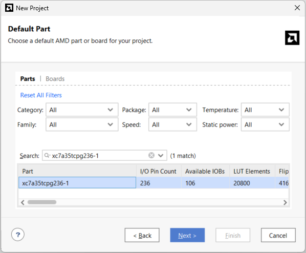
Select the FPGA part number of the FPGA on the Basys3 board in the catalog. This part number is xc7a35tcpg236-1, and can be found in the Basys3 reference manual \cite{Basys3Reference}. It is also partially written on the FPGA chip itself.
Press Next >.
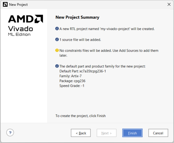
Press Finish to close the wizard and create the project.
Overview of Vivado
After closing the wizard, the window shown in Fig. 11 should appear. This window consists of a number of sub-windows, commonly called “panes” (Dutch: “ruit”).
Of these panes, the Flow Navigator (flow as in workflow) is the most important. The Flow Navigator is the pane from which you open different menus. For this tutorial the relevant menus are Project Management, Synthesis, Implementation and Program and Debug.

Figure 11:Main window of Vivado. All items and panes related to “Project Manager” in the Flow Navigator pane are inside the red selection.
For every Flow Navigator menu, the panes on the right might look slightly different. However, they are generally as follows:
Sources lists all user-created files that Vivado needs to do things. Vivado sees them as the “source” of the files it creates.
Properties shows the properties of the file that is selected in the Sources pane. Click on a file to select it.
Workspace shows information that is relevant to the menu selected in the Flow Navigator.
Results has a number of tabs with tools that help with debugging:
Tcl Console is a terminal that can be used to run interface with Vivado without using the GUI.
Messages is where Vivado shows any errors or warnings it encounters. If, for example, there is something wrong with your code, it will show up here.
Log tracks every important task that Vivado performs while it is running a routine.
Reports is a menu from which you can open summaries with information about the execution of a routine.
Design Runs shows the status and properties of a routine.
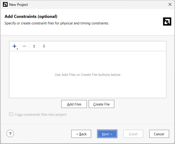
Step 3: Add Constraints
During synthesis Vivado will interpret your HDL source files and generate a circuit model from it. With the files that Vivado currently has, it cannot generate a complete model. It still misses knowledge of which port of the SystemVerilog module in “blinking_led.sv” should be connected to which FPGA pin, and how each pin should be configured. We do this by creating a Xilinx Design Constraint (XDC) file.
Click the “+” icon in the Sources pane. A wizard should pop up. Select Add or create constraints and click Next >.
In this next section of the wizard, click “Create File”. A pop-up should appear. Name your constraint file “blinking_led_constraints” and press OK.
Finally, press Finish to close the wizard. Your Sources pane should now look like Fig. 12.
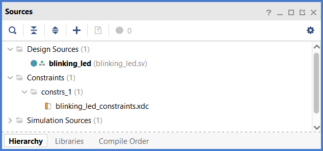
Figure 12:The “Sources” pane with the newly added constraint file (Flow Navigator > Project Manager).
The following XDC code associates the port called
clkin “blinking_led.sv” with FPGA pin W5, and configures it to use Low Voltage CMOS (LVCMOS) circuitry where binary 1’s are represented by 3.3 V.set_property -dict {PACKAGE_PIN W5 IOSTANDARD LVCMOS33} [get_ports clk]Add modified copies of the line above to connect port
rstto pin V17, portshortto pin V16 and portledto pin U16 as shown in Fig. 3.The following XDC code lets Vivado know that the port
clkis a clock. When Vivado knows this, it will allow the signalclkto use the dedicated clock circuitry on the FPGA.create_clock -add -name sys_clk_pin -period 10.00 -waveform {0 5} [get_ports clk]The following XDC code sets two parameters that Vivado wants to know to configure the FPGA. Technically, you could omit these lines, but Vivado will show a warning in the Messages tab in step 5 if you do.
set_property CONFIG_VOLTAGE 3.3 [current_design]
set_property CFGBVS VCCO [current_design]
Save your changes to the file.
Step 4: Synthesis
In this step we’re going to let Vivado synthesize a circuit model from the provided HDL code and constraints file.
In the Flow Navigator, click “Run Synthesis.” A window may pop up which you can simply close by clicking OK.
While Vivado is running the synthesis, go to the Design Runs tab in the bottom right. In this tab you can see when the synthesis has finished.
Once the synthesis is completed a confirmation pop-up appears saying “Synthesis successfully completed.” On the pop-up, select Open Synthesized Design and press OK. Alternatively, you can close the pop-up, and click Open Synthesized Design in the Flow Navigator.
Once Vivado has finished loading you can see from the Flow Navigator that Synthesis is now selected instead of Project Manager.
To view the synthesized model, click on Schematic under Open Synthesized Design in the Flow Navigator. The schematic shown in Fig. 13 should appear. Feel free to explore the schematic by zooming in (ctrl + scroll) on it and by double clicking the blocks.
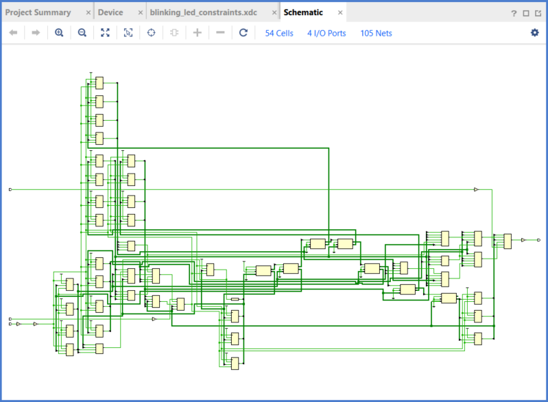
Figure 13:Schematic pane in Vivado
Step 5: Implementation
In this step we’re going to let Vivado create a circuit using the logic blocks on the FPGA.
Click on Run Implementation in the Flow Navigator. If a pop-up appears right after pressing Run Implementation, click OK.
By default a tab called Device opens with a schematic of the internal circuitry of the FPGA (See Fig. 14). Feel free to explore the schematic by zooming in (ctrl + scroll) on it and by clicking on blocks.
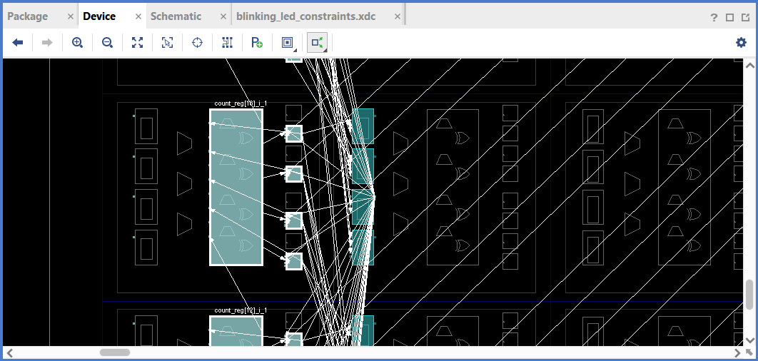
Figure 14:Device pane in Vivado after enabling Show Cell Connections (rightmost button in the Device pane) and clicking a logic block that is used in the circuit.
Step 6: Programming
In this step we’re going to let Vivado program the FPGA on the Basys3 board.
Get a robot.
Connect the Basys3 board to your PC with an USB-A to micro-USB cable. Connect to the highlighted USB port in Fig. 1.
Set the POWER jumper highlighted in Fig. 1 to USB. Now the board gets its power through the USB cable.
Switch the board on using the switch to the right of the POWER jumper.
In the Flow Navigator in Vivado under Program and Debug, click Generate Bitstream. Answer all pop-ups that may appear with OK.
After Vivado completes the bitstream generation, click Open Hardware Manager under Program and Debug in the Flow Navigator.
Click Open target in the green bar on top of the workspace pane (See Fig. 15) and choose Auto Connect. This will establish a connection between Vivado and the FPGA on the Basys3 board.
Click Program device in the green bar to configure the FPGA (See Fig. 16).
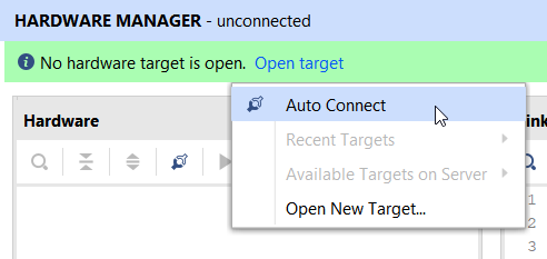
Figure 15:Open target button
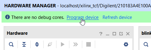
Figure 16:Program device button
Set both switch 0 and 1 on the Basys3 board low. LED 0 should now blink.
Set switch 1 high. LED 0 should have a shorter pulse duration.
Powering the FPGA from an External Power Source
So far the FPGA board has been powered through the USB cable that is also used to program the FPGA. The robot, however, is powered by a battery. To change the power source of the FPGA board to the battery, do the following:
Connect the battery to the robot, and switch the power board on.
To swap the power supply of the FPGA board to the battery, set the POWER jumper (See Fig. 1) to EXT (“external”). This external voltage isn’t exactly the battery voltage. The green power board extra circuitry to protect the FPGA board and to supply a stable 5 V.
You can see that the FPGA board is powered because the LED next to the POWER jumper is on. However, LED 0 isn’t blinking anymore. During the switching between power supplies the FPGA was briefly unpowered and lost its configuration data. This is because the configuration data that is uploaded to the FPGA through the USB cable is stored on the FPGA in an SRAM that is connected to the FPGA’s configuration circuitry. SRAM is a volatile type of memory. It loses its data when it gets no power.
Connect to the FPGA with Vivado’s Hardware Manager, as was done previously in step 6.
Program the FPGA with the same file. LED 0 should start blinking again.
Disconnect the USB cable. LED 0 should keep blinking.
Optional: Prevent the FPGA from Losing its Configuration Even If Power Is Off
To keep the configuration even when the FPGA board isn’t powered, the configuration can be uploaded to an external flash memory chip instead of the SRAM of the FPGA. Flash memory is non-volatile. When the board is powered on or when the process of uploading the configuration file has finished, the board sends the configuration from the flash memory to the SRAM of the FPGA.
To configure the board through flash memory, do the following:
In the Flow Navigator, go to Project Manager > Settings > Bitstream and check the option “-bin_file”. When you generate a programming file, Vivado will now create an additional file with the .bin extension. This file is used to program the flash memory.
Set jumper JP1 in the top right corner of the FPGA board (See Fig. 1) to the “SPI Flash” setting shown in Fig. Fig. 17.
In Vivado, go to Flow Navigator > Hardware Manager and right-click the FPGA serial number in the Hardware pane as shown in Fig. 18.
A window should pop up called “Program Configuration Memory Device.” Under the Memory Device option, select “s25fl032p-spi-x1_x2_x4”. The first part of this name is the serial number of the flash memory chip.
Click OK to close the window.

Figure 17:Different configurations for jumper JP1 \cite{Basys3Reference}.
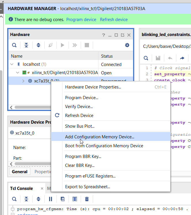
Figure 18:Add configuration memory device.
The flash memory should now be listed under the FPGA in the Hardware pane, as shown in Fig. 19. Right-click the flash memory and select “Program Configuration Memory Device...”
The “Program Configuration Memory Device” window should pop up. Click the 3 dots to the right of the Configuration file field and select the file “blinking_led.bin”. If you can’t find this file, it should be under ./tutorial_vivado/my-vivado-project/my-vivado-project.runs/impl_1/blinking_led.bin.
Click OK. The flash memory will now be programmed.
Once the programming has finished, press the PROG button in the top right corner of the board. If all went well, LED 0 will start blinking like before.
Turn the FPGA board off and on using the POWER switch in the top left corner of the board. The process of turning a device off and on is called power cycling. If all went well, LED 0 should be blinking again.
When you’re finished, set jumper JP1 back to the JTAG setting (see Fig. 17). In this mode the SRAM of the FPGA is programmed directly through micro-USB as was the case in the previous steps. In most cases you will encounter in your studies you don’t need to power cycle the FPGA board. Therefore, you are recommended to use JTAG programming by default. Flash memory programming is much slower, and should only be used when you really need non-volatile memory.
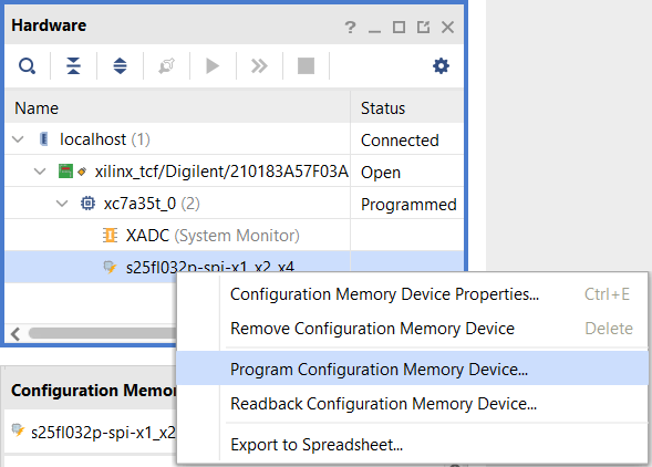
Figure 19:Program Configuration Memory Device window