Contactless Energy Transfer
General Introduction
Welcome to Contactless Energy Transfer part of the EE1L2 course! In this part of the course, you will be designing, testing, and improving a contactless power transfer system, in order to wirelessly transfer power to your group’s robot in the most efficient possible manner. This manual starts with a description of the practical, overall objectives, way of working, and time schedule.
Scope
The overall goal is to design, build, and test an electrical system for contactless power transfer. The duration of the practical is 6 weeks. Each week consists of two half-days in the Tellegen Hall and some self-study hours in order to prepare for the lab, aswell as report writing.
Educational Objectives
The overall learning objective of the practical is to apply and integrate the learned knowledge about power electronics in practice. More specifically to:
Develop and increase skills in designing, building, testing, measuring and debugging practical electrical systems.
Apply the knowledge from the Electrical Energy Fundamentals course: transformers and power converters (component choice, topologies, maximizing efficiency).
Report
The practical results are to be documented in a chapter of the final report for the whole Integrated Project 2. The report should document your design choices and the design itself of the contactless power transfer system as well as the measurement results, and how they compare to the design values. The focus should be on useful explanations about your findings, measurement results, and the conclusions you drew.
A suggested planning of the assignments is provided, but you can make your own planning as long as you meet the given deadlines in Time Schedule and Deadlines.
Facilities
Lab support
The practical is carried out at the Tellegen Hall, from weeks 2 to 8. The following support is available:
Student assistants; student assistants are your primary help. Assistants also check presence and verify your progression in the practical.
Hardware & Lab support; two staff members are responsible for monitoring the process, checking the results, and for problem solving in case the student assistants cannot solve them.
Rules & Regulations
Additional to the rules and regulations of the Practicumgroep EWI the following rules and regulations are applicable:
You may not work alone in the Tellegen Hall. A staff member or TA must be present at all times.
You are working with power electronics with high currents and/or voltages. This means that there are several additional safety regulations, see the items below:
Make sure that all the power sources are off and disconnected from your circuit, when you build or adjust a circuit.
When you build a new circuit, let the student assistant check your circuit before powering it up for the first time.
Contacts with a higher voltage must be shielded (i.e. placed in a provided metal box). This will be clearly stated in this manual.
Only work with dry hands, and always wear shoes.
Be careful with jewellery (e.g. rings, necklaces, bracelets, watches), they conduct.
Do not use cables with bad or damaged insulation.
If someone gets an electric shock, turn off the power and call a support staff member.
In case of emergency (serious injury to people or objects), press the red emergency button and call a staff member for help.
If first aid is needed, Ton Slats (room LB01.260) or Martin Schumacher (room LB01.271) can help.
The emergency phone number with a TU Delft telephone is 112. When you call with your mobile phone, dial 015 27 81226 to be redirected to the TU Delft emergency center.
Overview
You are going to investigate, design, build, and test a method of contactless transferring power. The overall system implementation can be approached in a couple of steps:
Design, build, and test the DC/AC-inverter.
Design, build, and test the AC/DC-rectifier.
Design, build, and test an air-core transformer.
Investigate the possibility of contactless power transfer with the air core transformer.
Learn how to compensate the air core transformer (i.e. improve the power factor) to enable it to transmit a considerable amount of power at its resonant frequency.
Test and evaluate the complete power transfer system and measure the efficiency.
Implement the overall system on the robot and optimize the power transfer.
Time Schedule and Deadlines
The practical has 6 scheduled lab weeks in Q4. This section shows a suggested time planning regarding the steps mentioned previously, such that you can meet the deadlines.
| Week | Activities |
|---|---|
| 4.2 | Steps 1 & 2: Start on the design of both converters (i.e. inverter and rectifier). |
| 4.3 | Steps 1 & 2: Hand in the schematic design and start assembly of both converters. |
| 4.4 | Steps 1 & 2: Test and perform measurements on both converters. |
| 4.5 | Steps 3 & 4: Designing, building and evaluation of the air-coupled transformer (i.e. coils). |
| 4.6 | Steps 4 & 5: Theory and calculations on compensation of the air-coupled transformer. |
| 4.7 | Steps 6 & 7: Performance measurement on the complete system. |
| 4.8 | Deadline Deliverable Reports |
Converter Design for Contactless Power Transfer
Learning objectives: The following will be learned and practiced in this chapter:
Designing a top-level circuit schematic based on available components and their data-sheets.
Understanding the function of the sub-circuits and connecting them to obtain the full converter (excluding the air coupled transformer).
Choosing specific circuit components based on data-sheets.
Assembling and soldering a (power) electronics circuit.
Testing and debugging an electrical circuit step by step to ensure desired operation.
Deliverable: A basic top-level schematic design of the inverter and rectifier plus a functioning prototype.
Time duration: Two lab sessions for the design and two/three for building and testing.
Task Description
The task of this chapter is to understand the role of each sub-circuit and connect the sub-circuits into the full DC-DC converter design (excluding the air coupled transformer). Choose among provided components on Brightspace to draw a schematic design for both the AC-DC rectifier and DC-AC inverter. Build, solder, and test both converters on the provided PCBs to obtain a fully functioning prototype.
Information on the DC-DC Converter
The electronic system as shown in Fig. 1 consists of three main parts, a DC-AC converter (i.e. inverter), a high frequency air coupled transformer (i.e. coils) and an AC-DC converter (i.e. rectifier). Furthermore, there are additional sub-circuits for driving the switches and overall circuit protection (not shown in the figure). In this chapter you need to design, build and test both the inverter and rectifier.
In order to come up with the schematic design for these, a number of preselected components is made available. Their datasheets can be found on Brightspace, and some are elaborated on in the next sections. Try combining these with the knowledge learned during lectures of the Electrical Energy Fundamentals Course on the different converter topologies.
Think carefully about how you would do this, following the guidelines at the end of the chapter and ask the hardware support or consultant if you have any doubts or questions!

Figure 1:The DC-DC converter for contactless power transfer.
The operating condition of the converter is 18V and 3A; keep this in mind when selecting components.
Diode parameters
Read through the datasheets and try to figure out which parameters matter the most to your design.
MOSFET parameters
So far in our analysis of power electronic circuits it was assumed that all switches (i.e. transistors) are ideal. That is, they switch instantaneously between ON and OFF states without delays, signal generation effort, or transition losses. You will have several options available for choosing the MOSFETs for the inverter circuit. They differ in switching times and losses when conducting current (e.g on-resistance).
The PWM generation and control circuit
A MOSFET requires a voltage in its gate and source terminals to operate. In power electronics, N-channel MOSFETs are commonly used. For simplicity, whenever “MOSFET” is mentioned in this manual, it refers specifically to an N-channel MOSFET, unless stated otherwise.
To control the switching behavior, a type of signal called a pulse-width modulated (PWM) signal is used. There are several ways to generate PWM signals one example is shown in Fig. 2. Although it is possible to build a PWM generator using discrete components like transistors and operational amplifiers, it is more practical to use a dedicated integrated circuit (IC) or microcontroller.
In this lab the LAUNCHXL-F28027F development board from Texas Instruments will be used, which is equipped with a microcontroller capable of generating the required PWM signals.

Figure 2:Generating the PWM switching signals for the full bridge converter
Gate driver (IRS2001PBF)
The PWM signal generated by the control circuit typically lacks sufficient power to drive the MOSFETs directly. Therefore, an intermediate circuit—known as a gate driver is required between the PWM source and the MOSFETs.
Another key challenges in gate driving arises from the difference between low-side and high-side MOSFETs in an H-bridge configuration. Driving the low-side MOSFET is relatively straightforward, as their source terminals are referenced to ground. However, driving the high-side MOSFET is more complex because their source terminals are not grounded and can float to various voltage levels even being equal to the supply voltage.
To ensure proper operation, a special gate-driver circuit is needed that can deliver and maintain a voltage equal to or greater than the required turn-on threshold between the gate and source of the high-side MOSFET—regardless of its source potential. This includes worst-case scenarios where the source is at the same potential as the positive supply rail, such as when the high-side MOSFET is fully ON.
The datasheet of the used gate drive integrated circuit is found on Brightspace. This gate drive circuit is able to deliver and keep the required voltage under all operating conditions. Furthermore, the gate drive circuit can deliver a current of compared to of the LAUNCHXL-F28027F.
Guidelines
You can use the following guidelines to help you achieve the objectives of this chapter:
Begin by designing the rectifier schematic to become familiar with datasheets and component selection (e.g., diodes).
Design the top level circuit diagram for a H-bridge inverter with datasheets and component selection (e.g., MOSFETs)
Go deeper in the inverter design starting with the 2 inverted PWM signals to the gate-drivers to the MOSFETs.
Discuss the circuit schematics you designed with the hardware support. After approval, you will receive the PCB for the inverter and rectifier.
Check your progress with a TA
Assemble and test only the “Conversion” and “LV system” circuit parts of the inverter; this includes the 5 V and 3.3 V regulators, and all of their surrounding components. Also, solder on the V+ and GND connector. Leave the 3 headers for the TMS320f2807f Launchpad and the entire gate driver part of the PCB unpopulated.
To power the inverter, use the bench power supply with 18 V supply and set a current limit to about 0.5 A
and should be present on the test-points. You can use a multimeter to check this.
Check your progress with a TA
Assemble the TMS320f2807f Launchpad pins on the inverter. In order to align the connectors of the development-board, use the dummy board.
Recheck if and still work, without the dummy board.
If both still work ask support staff inorder to obtain a working development-board.
Check your progress with a TA
Test the push buttons and see what it does with the red LED on the PCB.
Investigate the behavior of the “Low Voltage” circuit by measuring the PWM waveforms using an oscilloscope whilst varying the duty-cycle and switching frequency using the variable resistors. Be careful not to break these. How do the acquired waveforms compare to Fig. 2? Are the parameters what you expect?
Check your progress with a TA
For now, set the frequency to 100 kHz and the duty-cycle to your choice for the optimal value.
Assemble the rest of the inverter (e.g. the “High Voltage” circuit). Carefully make sure all component orientations are correct and no short circuits are made. Do not turn on the converter!
Investigate the behavior of the inverter by inserting it in the metal enclosure and connecting it to the resistive load (a 10 ohm resistor with an heatsink). Set the bench power supply voltage to 18 V and the current limit to 3 A. Then use the oscilloscope to obtain the wave-form over the load. Write down and explain your findings.
Check your progress with a TA
Assemble the rectifier circuit, carefully watch the orientation of the diodes. After assembly, insert it in its metal enclosure.
Think of an easy but effective way to test the rectifier, where did you design it for? Write down and explain your findings.
Check your progress with a TA
Obtain an efficiency and power score for your system at the dedicated measurement setup operated by one of the Lab support.
Air-Coupled Transformer Design for Contactless Power Transfer
Learning objectives: The following will be learned and practiced in this assignment:
A revisit of the theory of coupled inductors.
An alternate measuring technique of the coupled inductor parameters using specialized equipment.
Designing and building an air coupled transformer.
Deliverable: A functioning air-coupled transformer usable in the overall system.
Time duration: One or two lab sessions.
Task Description
Design and build an air-coupled transformer for the DC-DC converter. Determine the coupling coefficient and other electrical parameters of the air-coupled transformer with various separation distances. Analyze the power transfer characteristics of the air-core transformer system. Evaluate the operation of the DC-DC converter combined with the air-coupled transformer.
Information on the Air-Coupled Transformer
For the contactless power transfer an air-core transformer will be used. As with any transformer the system consists of two coupled inductors. However, the main difference is the absence of a well-defined magnetic circuit. This lack of a low-reluctance path for the magnetic flux to couple the primary and secondary windings together results in a magnetically loosely coupled system.
Winding of the coils

Figure 3:Basic shape of the contactless power transfer coils
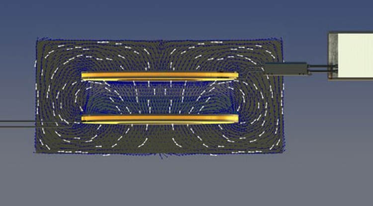
Figure 4:Basic shape of the contactless power transfer coils
The basic shape of the winding that will be used is shown in Fig. 3. Having this flat shape allows for a little more flexibility in the setup of the contactless power transfer. If the coils are made long and slim instead of flat and wide (as the one shown in Fig. 3) then the alignment of the coils would be more difficult.
To illustrate this point, consider Fig. 4, here two coils of the shape of Fig. 3 are placed above one another and the distribution of the magnetic flux is superimposed on the image. Although it can be seen that there is a fair amount of flux generated by the coil in the bottom that does not couple with the coil on top, it can also be seen that the relatively flat shape of the coil helps to capture as much flux as possible.
Coil parameters
You will design and wind your own coils. First consider the design constraints. The inside diameter of both coils should not be smaller than 5cm. A small inside diameter not only limits the ability of the coil to capture flux but the inner winding also contributes little to the inductance. The total inductance of the larger coil (i.e. primary coil) should be approximately 100 μH and 20 μH for the smaller coil (i.e. secondary coil).
Litz wire
A special type of high frequency wire, called Litz wire, that consists of many small insulated strands bound together will be supplied for the coils. The total inductance and the length of wire needed can be estimated using the air-core inductance calculator found at http://
Coil theory and measurement methods
Consider the coupled inductors shown in Fig. 5. Let and be the self inductance of the two coils and be the mutual inductance of the two coils. From previous courses it is already known that we can model this circuit with:
where the following holds for :
where is the coupling factor.

Figure 5:Two coupled inductors


Consider the circuits shown in Fig. 6 & 7. The inductors are connected in series in both circuits, however, in the one instance the induced voltages are in the same direction while in the other they oppose one another. Measuring the inductance of these circuits as well as the self-inductances of and gives enough information to calculate the coupling coefficient.
Lets define to be the total inductance of the two coils connected in the series aiding configuration. Finally, let be the total inductance of the two coils connected in the series opposing configuration.
When the two coils are connected in series (irrespective of whether they are connected in the aiding or opposing configuration) they share the same current, . If is the voltage across and is the voltage across the following can be written when the coils are connected in the series aiding configuration:
Using these equations one can calculate the voltage across the two coils when connected in the series aiding configuration, , as:
Since the voltage across the the two coils connected in the series aiding configuration is related to the total inductance of the two coils as:
You now know that:
You can prove that for the series opposing connection of the two coils the total inductance of the two coils are:
Using these equations you can now calculate the mutual inductance as:
And since:
One can now calculate the coupling coefficient .
In this discussion you have made a number of simplifying assumptions, most notably you have ignored the winding resistances. Although this simplified model gives you enough information to understand the operation of the system, it can not describe all the behavior of the system.
Power transfer characteristics of the coil
Consider the coupled inductor circuit shown in Fig. 8. Since you are interested in the fundamental component you can assume that the frequency of the source is 100 kHz. Recall that for the coupled inductors you can write the following equation, in the frequency domain:
Using this expression you can write the Kirchhoff voltage loop law equations for the system in Fig. 8 as:

Figure 8:Basic coupled inductor power transfer circuit
If you solve this equation, only a small amount of power is transmitted to the load resistance if the coupling coefficient is low, as can be seen in the following equation:
Guidelines
You can use the following guidelines to help you achieve the objectives of this chapter:
Design and the primary and secondary coil of the air coupled transformer, based on the requirements set in Coil parameters.
Check your progress with a TA
After submitting your design and obtaining the Litz wire, wind both of the coils. \textbf{When the winding process is done, ask a TA to pre-tin your coils.} You will need to explain why this is needed, thus do some research prior to this.
Measure the parameters of the air coupled transformer for separation distances of 2, 4, and 6 cm, using the specialized LCR-meters in the Tellegen Hall. Write down your findings and calculations.
Using these findings, analyze the power transfer of the circuit. Calculate the power supplied to a load of 10 Ω and the efficiency. You can assume a 18 V, 100 kHz source.
Check your progress with a TA
Place the air coupled transformer into the DC-DC converter with 2 cm distance between the coils. Set the powersupply to the same settings as before, thus 18 V and 3 A.
Measure the waveforms of the converter, the primary coil current, secondary coil voltage and the load voltage. How much power can be delivered to a 10 Ω load? And what is the efficiency. Write down your findings.
Check your progress with a TA
Obtain an efficiency and power score for your system at the dedicated measurement setup operated by one of the TA’s.
What You Should Know
Upon having successfully performed this chapter and studied the required theory, you should be able to answer the following questions:
Discuss the method used to determine the mutual inductance using the series opposing and series aiding method.
How does the mutual and magnetizing inductance change with an increase in separation distance? Explain.
The problems with delivering power with an uncompensated air core transformer.
You can reflect on some of these questions in the report.
Compensation of the Air-Coupled Transformer
Learning objectives: The following will be learned and practiced in this assignment:
Analysis of the resonant compensated transformer circuit.
An investigation into possible fault modes.
Practical implementation and verification.
The operation of over-current system protection and testing the circuit for correct operation.
Deliverable: Functioning compensation network and tuning.
Time duration: One or two lab sessions.
Task Description
A method of compensating the unwanted characteristics of the air-coupled transformer is to be analyzed and implemented, thus massively increasing the effiency of the system. When this compensated system is operating under certain conditions the system might fail due to overcurrents. This failure mode and the systems protection circuitry against this error mode is described and must be tested.
Information on Compensating an Air-Coupled Transformer
In the previous chapter, whilst analyzing the air-coupled transformer, you have seen that the power transfer characteristics of such a transformer are poor, because the power factor is very low. In this chapter, you will look into a solution to this problem.
Compensation capacitors
A common approach to improve the power factor of the inductive circuit is adding so called compensation capacitors. As shown in Fig. 9., capacitors and are added in series to the primary and secondary circuit respectively. Similarly to Power transfer characteristics of the coil., by applying the Kirchhoff’s law, you can now write:

Figure 9:Compensated coupled inductor power transfer circuit
The Thévenin’s equivalent impedance of the primary side is calculated as:
In order to transfer power at optimal efficiency, the Thévenin’s equivalent impedance should only have real component. Therefore, the two components in (14). both should be 0, which gives:
As you can see, and are now resonant with and respectively at frequency . Then the primary side Thévenin’s equivalent impedance becomes:
Now let’s calculate the power transfer efficiency of the above depicted fully compensated circuit. The primary current can be written as:
Substitute (17) and (15) into (13) you obtain the secondary current as:
The output power is then calculated as:
Optimal switching frequency
If we consider the coil resistances and , the total input power can be approximated as:
The power transfer efficiency is:
As can be seen, the efficiency reaches the maximum when the denominator is minimal, which happens when:
The above equation can be used to choose optimal switching frequency to maximise power transfer efficiency for a given load resistance , mutual inductance , and coil resistances and . Note that and are actually ac resistances, which differ from dc resistances because of high frequency effects, specifically skin effect and proximity effect.
Coil misalignment
The other problem for the fully compensated case is the misalignment of the coils. Consider what would happen if the secondary coil is removed from the primary coil or the two coils are heavily misaligned. The mutual inductance becomes close to 0. According to (17)., the primary side current will be extremely high since the equivalent impedance is too low. Large currents may damage the inverter circuit. Therefore, an over-current protection circuit is included. Its datasheet is available on Brightspace and should be studied.
Guidelines
You can use the following guidelines to help you achieve the objectives of this chapter:
Use the theorems presented in this chapter to calculate your optimal switching frequency.
Use the theorems presented in this chapter to obtain your compensation circuit values for both converters.
Using the theorems presented in this chapter and your found compensation circuit, calculate the power supplied to a load of 10 Ω, and efficiency of the circuit.
Check your progress with a TA
Using the available capacitors, assemble your compensation circuit on both PCB’s.
Test the compensated overall system. Adjust the frequency and receiver coil position to match the optimal values determined in the previous steps. Measure the power delivered to the load and compare it to that of the uncompensated system. Document your observations and provide explanations.
Check your progress with a TA
At last, you can obtain an efficiency and power score for your system at the dedicated measurement setup.
What You Should Know
Upon having successfully performed the steps from this chapter and studied the required theory, you should be able to answer the following questions:
Why you can estimate how the air core transformer will react when connected to the inverter by investigating its operation with a 100 kHz sinusoidal source.
How to compensate an air core transformer and why this works.
The potential problem with this compensated system.
How the inverter circuit is protected against this fault. You must be able to explain in detail how this works and also be able to give an estimate of the current level where the current protection circuit will trigger.
Integration of the System on the Robot
Learning objectives: The following will be learned and practiced in this chapter:
Integrating power electronics in an embedded system.
Gaining insight into the influence of coil alignment and switching frequency on the power transfer of an air-core transformer system.
Experiencing how real-time adjustment of position and frequency can maximize transferred power in a contactless charging setup.
Collaborating with fellow students on one project.
Deliverable: A fully integrated contactless power transfer system on the robot that enables real-time adjustment of coil position and inverter switching frequency to maximize transferred power during the maze demonstration.
Time duration: One or two lab sessions.
Task Description
To integrate the developed contactless power transfer system onto the robot used for the Integrated Project 2. Optimizing power transfer using the robot’s placement.
Robot demonstration
To demonstrate the principles of contactless power transfer, you will attach the secondary coil to the robot and connect it to your rectifier, thereby using the car’s headlights as a load.
During the demonstration, the inverter and primary coil are placed in the maze. The robot drives backwards to the charging spot. Real-time adjustments of coil position and inverter switching frequency are performed to maximize transferred power. The robot’s LCD display shows the current received power and indicates when the battery is fully charged (flashing battery symbol). When the battery symbol starts flashing, the robot may begin the rest of the maze. The amount of time this takes depends on how much power you can transfer.
Collaboration with the Robot Control Group
This chapter requires close collaboration with the group responsible for the robot’s control system (the robot control group). They handle robot movement (including backwards driving and position adjustments) and issuing the start command for the maze. Your group (power transfer) provides the inverter with a real-time frequency control interface and ensures the system achieves high power transfer when properly aligned. Joint testing and demonstration are essential for success.
Communication with the Inverter and Robot
The inverter switching frequency can be adjusted in real-time via USB serial commands from a laptop:
The LAUNCHXL-F28027F LaunchPad on the inverter PCB is connected via micro-USB to the control laptop.
Baud rate: 9600, 8N1.
Command (terminated with \n): FREQ:xxxxx, where xxxxx=frequency in Hz (valid range: 80000 to 120000 Hz).
Power monitoring
Transferred power is measured on the robot side and displayed in real-time on the robot’s LCD display (current received power and battery status). Additionally, this data is sent to a web page (hosted on a central server) that is crucial for the control laptop to monitor the current power transfer level. This web page is used to guide real-time adjustments of position and frequency to achieve maximum efficiency. If you use device 1 (number is on the usb port), the measured powertransfer can be read by the following url: https://
Usage during the maze test
The robot is positioned in front of the charging spot and has to backup into the charging spot.
The control laptop monitors the current received power via the web page.
Position and frequency are adjusted in real-time based on the web page data to achieve the highest possible power transfer.
The robot’s LCD display shows the current power and flashes the battery symbol when charging is complete. When the battery symbol flashes, the robot may begin the rest of the maze.
Guidelines
You can use the following guidelines to help you achieve the objectives of this chapter:
Securely attach the small coil to the back of the robot car using the supplied plastic butterfly nuts. Ensure the coil is firmly in place to prevent any disconnection during operation.
Insert the rectifier into the metal clip located on the robot car. Connect the output terminals of the rectifier to the input terminals of the board equipped with lights.
Test the setup with your inverter and secondary coil. The lights should turn on.
Test the complete setup in the maze.